Siltronic breaks ground for a new fab in Singapore
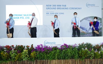
Munich/Singapore, October 26, 2021 – Siltronic, one of the technology leaders in silicon wafer manufacturing, broke ground for its new manufacturing facility at JTC’s Tampines Wafer Fab Park in Singapore. In partnership with the Singapore Economic Development Board (EDB), Siltronic’s investment of around EUR 2 billion (equivalent to nearly SGD 3 billion) until the end of 2024 will play an important role in meeting the growing semiconductor demand.
Singapore’s Minister for Trade and Industry, Mr. Gan Kim Yong was the Guest-of-Honour at the ground breaking ceremony. He was accompanied by Siltronic CEO, Dr. Christoph von Plotho, EDB Managing Director, Ms. Jacqueline Poh, and Siltronic Site President in Singapore, Mr. Niew Bock Cheng.
“We support the expansion plans of our valued customers by adding a new 300 mm fab in Singapore. With the decision to invest in this cost-efficient facility, we are setting the course for Siltronic’s continued successful future.”, says Christoph von Plotho.
The global demand for semiconductor devices is growing continuously. Silicon wafers are the base material for these devices. Wafer supply is already tight and is expected to become even tighter in the next years. In order to meet the increasing customer demand, Siltronic will expand its capacity as existing fabs are already fully utilized.
Siltronic started its operations in JTC’s Tampines Wafer Fab Park in 1999 with the manufacturing of 200 mm silicon wafers. In 2006, Siltronic added a second fab under a joint venture with Samsung Electronics for the manufacturing of 300 mm silicon ingots and wafers.
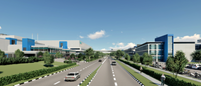
The new 300 mm fab under the joint venture with Samsung will be the most advanced wafer facility of the Siltronic Group, producing crystal ingots as well as polished and epitaxial wafers. It will strengthen Siltronic Singapore as a key production hub within Siltronic’s production network. About 600 new jobs for professionals, engineers, technicians and skilled workers will be created.
“This is the largest investment in the history of Siltronic. With the new leading-edge production capacities, we will further strengthen our position as one of the technology leaders. This investment also demonstrates our long-term commitment in Singapore.”, continues von Plotho.
Ms Jacqueline Poh from the EDB added: “We are committed to support the growth of the semiconductor industry in Singapore with industry leaders like Siltronic. Siltronic’s decision to site its largest and most advanced manufacturing facility in Singapore is a testament to our attractiveness as a global node for semiconductors. The new fab will further strengthen our semiconductor industry and create good job opportunities in Singapore.
Contact:
Dr. Rupert Krautbauer
Head of Investor Relations & Communications
Tel: +49 (0)89 8564 3133
E-mail: investor.relations@siltronic.com

