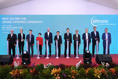
Siltronic AG celebrates the inauguration of the new fab in Singapore
Singapore, June 12, 2024 – Today marks a milestone in the history of Siltronic AG: After more than 500 construction days and roughly 23 million working hours, Siltronic inaugurated one of the world’s most advanced wafer fabs. The inauguration of the new production facility, which is one of the most modern and cost-efficient of its kind, took place today.
The highly automated fab at JTC’s Tampines Wafer Fab Park was officially opened in the presence of around 150 guests, including numerous high-ranking representatives of the Singaporean government, customers and suppliers. Singapore’s Deputy Prime Minister Heng Swee Keat was the Guest of Honour to grace the occasion. The fab was commissioned at the beginning of 2024 and will now be ramped to full capacity over several years.
"With our new fab, we will accompany the future growth of the wafer industry for many years to come and take Siltronic to a new level. What the entire team, including all business partners, has achieved is a masterpiece, and I would like to thank everyone for their outstanding contribution," said Dr. Michael Heckmeier, CEO of Siltronic AG, in his speech.
Ms. Jacqueline Poh, Managing Director of Singapore Economic Board (EDB) said: “We are proud of our long-standing partnership with Siltronic. As one of top 5 global wafer suppliers, Siltronic’s new fab is a significant expansion that not only supplies to Singapore’s semiconductor industry but also strengthens the resilience of the global semiconductor supply chain. This investment will create good jobs and further grow the existing collaboration that Siltronic has with local suppliers in automation and precision components.”
The success story of Siltronic in Singapore began in 1997 with the founding of Siltronic Singapore Pte. Ltd. in JTC’s Tampines Wafer Fab Park. The first 200 mm wafers were produced as early as 1999. This was followed in 2006 by the establishment of a joint venture with Samsung and the start of construction of the first 300 mm fab, from which the first wafers were delivered to customers in 2008. The foundation stone for the second 300 mm fab was laid in 2021, and it was officially opened today. Singapore is Siltronic's largest production site.
Today's inauguration of the state-of-the-art wafer fab in Singapore is not only the largest investment in Siltronic's history, but also a milestone of which Siltronic is extremely proud. With its high level of automation and impressive efficiency, the fab sets new standards in our industry and strengthens Siltronic’s position as one of the world's leading wafer manufacturers.
Contact:
Verena Stütze
Head of Investor Relations & Communications
Tel.: +49 89 8564 3133
E-mail: investor.relations@siltronic.com
Company profile:
As one of the leading wafer manufacturers, Siltronic is globally oriented and operates production sites in Asia, Europe, and the USA. Silicon wafers are the foundation of the modern semiconductor industry and the basis for chips in all electronic applications – from computers and smartphones to electric cars and wind turbines. The international company is highly customer-oriented and focuses on quality, precision, innovation, and growth. Siltronic AG employs around 4,500 people worldwide and has been listed in the Prime Standard of the German Stock Exchange since 2015. Siltronic AG shares are included in both the MDAX and TecDAX stock market indices.
